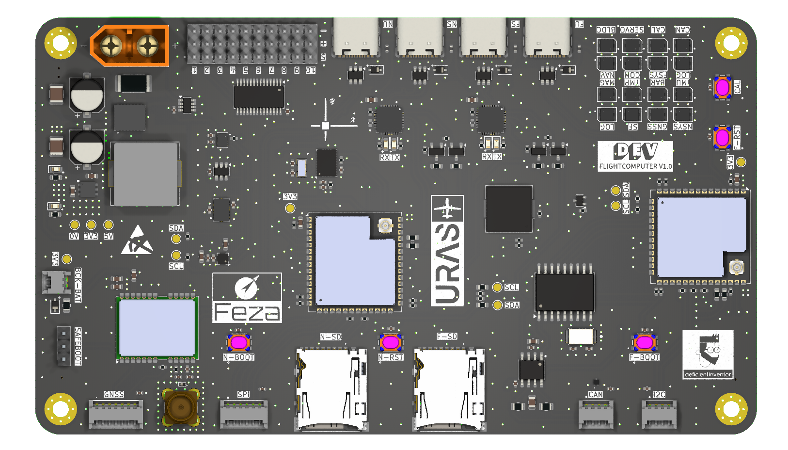
DEV Flightcomputer V1.1 (REV1)
Revision 1 documentation.
- You can easily navigate through the contents navigation bar on the right side.
- If you want to read about the design choices and overall system design, click here 🚀.
Revision Changelog
Change 1
Description:
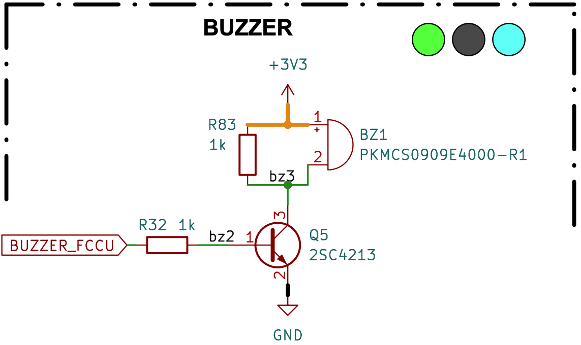
A transistor and two 1kΩ resistors were added to the buzzer circuit to protect the ESP32 and provide better control over the buzzer.
Changes:
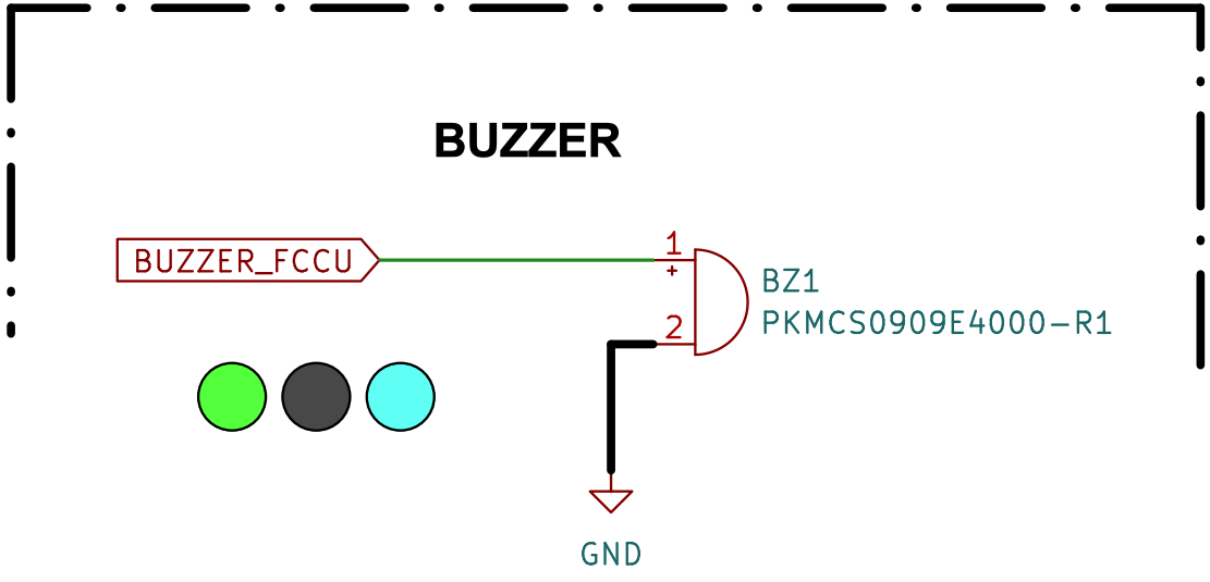
Before (Rev0):
The buzzer was directly connected to the ESP32 GPIO pin, which could lead to potential overload or insufficient control.
After (Rev1):
A transistor is now used to decouple the buzzer’s current path. Two 1kΩ resistors were added: one as a base resistor to limit the current to the transistor and another to control the buzzer’s operating current.
Improvements:
- ESP32 Protection: Prevents GPIO pin overload by offloading the buzzer’s current through the transistor.
- Improved Control: Ensures reliable switching of the buzzer with the transistor acting as an intermediary.
- Signal Stability: Controls the base current with a dedicated resistor, ensuring stable transistor operation and protecting the control circuit from malfunctions.
Change 2
Description:
Proper length matching of USB D+/D- lines is essential to ensure signal integrity and reliable communication. Adjustments were made to address trace length differences and optimize routing.
Calculation:
Parameters:
- \(L_{\text{Diff}}\): Maximum length difference between the traces (e.g., in mm or inches).
- \(S_{\text{Limit}}\): Skew limit in time (e.g., in ps or ns).
- \(\tau_{\text{Delay}}\): Delay per unit length.
- \(v_{\text{Signal}}\): Signal velocity in m/s.
- \(c\): Speed of light in a vacuum (\(3 \times 10^8 \, \text{m/s}\)).
- \(D_k\): Relative dielectric constant (FR4).
Combining the Formulas:
1st Substituting: \(\tau_{\text{Delay}} = \frac{1}{v_{\text{Signal}}}\) into the formula for \(L_{\text{Diff}}\):
\[L_{\text{Diff}} = S_{\text{Limit}} \times v_{\text{Signal}}\]2nd Substituting: \(v_{\text{Signal}} = \frac{c}{\sqrt{D_k}}\) into the formula for \(L_{\text{Diff}}\):
\[L_{\text{Diff}} = S_{\text{Limit}} \times \frac{c}{\sqrt{D_k}}\]Example:
Given:
\(S_{\text{Limit}} = 100 \, \text{ps} = 100 \times 10^{-12} \, \text{s}\)
\(D_k = 4.74\)
\(c = 3 \times 10^8 \, \text{m/s}\)
Calculation:
Result:
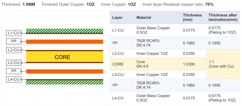
The maximum length difference \(L_{\text{Diff}}\) for a skew limit of 100 ps and \(D_k = 4.74\) is approximately 13.78 mm. This value includes the USB-Cabels and other PCBs.
Changes:
Before (Rev0):
One of the USB data lines had a 5mm longer trace and was routed underneath the ESD protection chip to avoid using vias. This length difference could result in signal degradation and timing mismatches.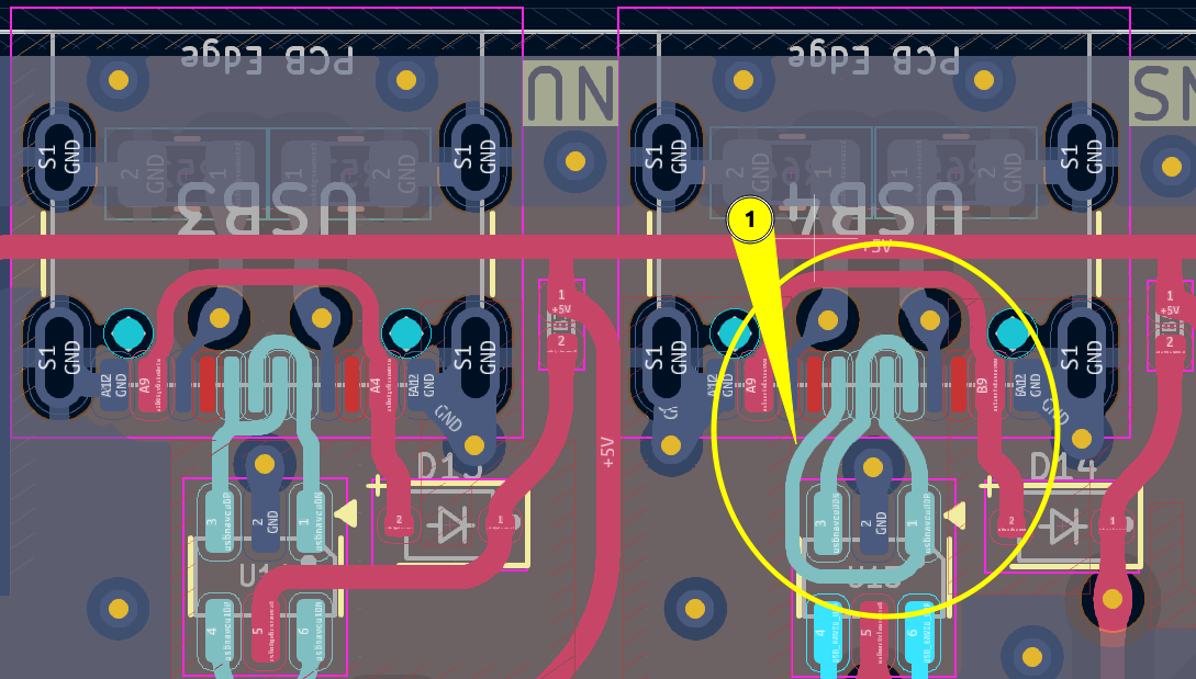
After (Rev1):
Vias are now used to route the USB data lines, reducing the length difference to just 1mm and achieving proper length matching. This change ensures compliance with high-speed USB design guidelines.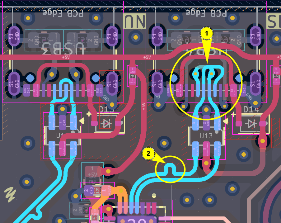
Improvements:
- Signal Integrity: The improved length matching enhances USB signal quality and minimizes timing issues, ensuring more reliable communication.
- Reliability: The routing adjustments maintain the effectiveness of the ESD protection chip while avoiding potential signal disruptions.
- Performance: By adhering to USB length matching requirements, the design supports high-speed data transmission with reduced risk of errors.
Change 3
Description:
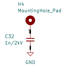
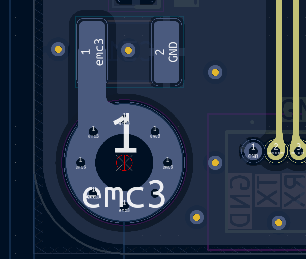
Added 1nF/2kV capacitors to each mounting point (Electromagnetic Compatibility).
Changes:
Improvements:
- Improved electromagnetic compatibility (EMC) and protection against external interference by adding 1nF/2kV capacitors to the mounting points. This helps reduce the impact of high-frequency noise and enhances the overall stability of the system.
Change 4
Description:
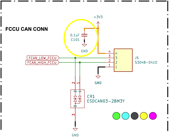
Added 100nF capacitors to all board-to-wire connectors.
Changes:
Before (Rev0):
No capacitors for the outgoing 3.3V pins of the board-to-wire connectors.
Improvements:
- Enhanced stability and noise reduction by adding 100nF capacitors to all board-to-wire connectors. This modification helps in filtering high-frequency noise and stabilizing the voltage supplied to the connected components.
Change 5
Description:
Updated the impedance calculations for the RF traces (GNSS).
Changes:
Before (Rev0):
Microstrip 50Ω Trace Width: 0.327 mm (calculated)After (Rev1):
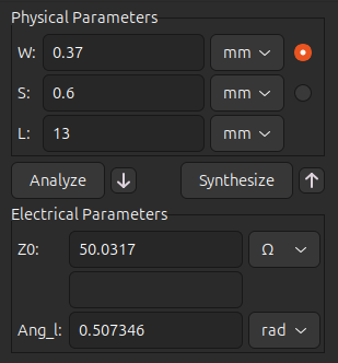
Coplanar Waveguide with Ground Plane 50Ω Trace Width: 0.37 mm (calculated)
Improvements:
- The coplanar waveguide (CPW) design is generally better for RF traces. In this revision, I corrected my previous mistake, where I had designed the trace as a CPW-WG but mistakenly calculated the impedance as if it were a microstrip. go to calculation🧮
Schematic
- You can access the PDF via the attached link or the PDF viewer.
Schematic Colored
Schematic Monochromatic
Trace’s / Impedance / Board
Power
| TraceID | TraceWidth (mm) |
|---|---|
| VBAT | 2.5 |
| +5V | 0.5-2.5 |
| +3V3 | 0.5 |
| REG_FB | 0.35 |
| GND | 0.5-4 |
Signal
| TraceID | TraceWidth (mm) | Spacing (mm) | Impedance (Ω) |
|---|---|---|---|
| SPI | 0.327 | 0.6 | 50 |
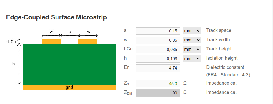
| USB | 0.35 | 0.15 | 90 |
| UART | 0.327 | 0.6 | 50 |
| I2C | 0.327 | 0.6 | 50 |
| SIGNAL | 0.327 | 0.6 | 50 |
| RF | 0.37 | 0.6 | 50 CWG w/ Ground |
Calculations
50 Ω Coplanar Waveguide w/ Ground
50 Ω
90 Ω
Board
| Boardfinish | ENIG |
| Tented Vias | YES |
Gerbers as SVGs / ZIP
- For better visibility, open the SVGs in a new tab by right-clicking and selecting Open pic in new tab.
Layer 1 (SIG)
Layer 2 (GND)
Layer 3 (PWR)
Layer 4 (SIG)
Gerber Viewer & Download
- To use tracespace.io, click the settings wheel and set the use outline layer for board shape GAP FILL LIMIT to 0.25mm for an error-free board view.
Fabrication Document
Assembly Document
Bill of Material
Interactive BOM
- In case you prefer to use the fullscreen iBoM, you can acces it via the Settings Gear.
Costs
| Item | Price |
|---|---|
| Components | 150,27€ |
| PCB Manufacturing | 106,51€ |
| PCB Assembly | 29€ |
| TOTAL | 285,78€ |
 pie
    title Cost Breakdown
    "Components: 150,27€" : 150.27
    "PCB (5): 106,51€" : 106.51
    "Assembly (1): 29€" : 29
Reports
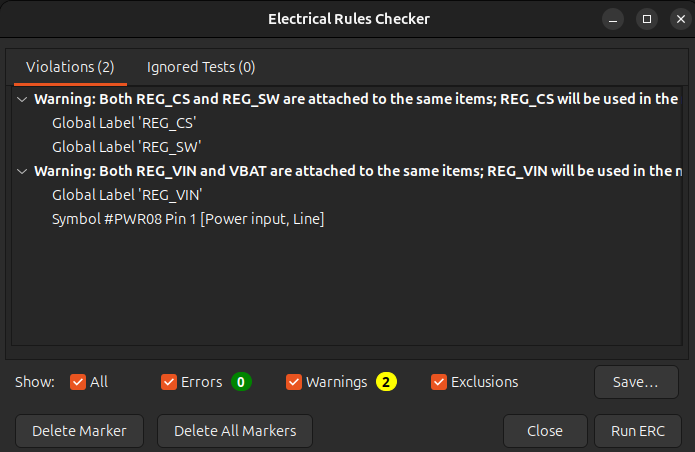
- The warnings from the ERC are known and occur due to the INA219 Current Sensor but the connections are right.
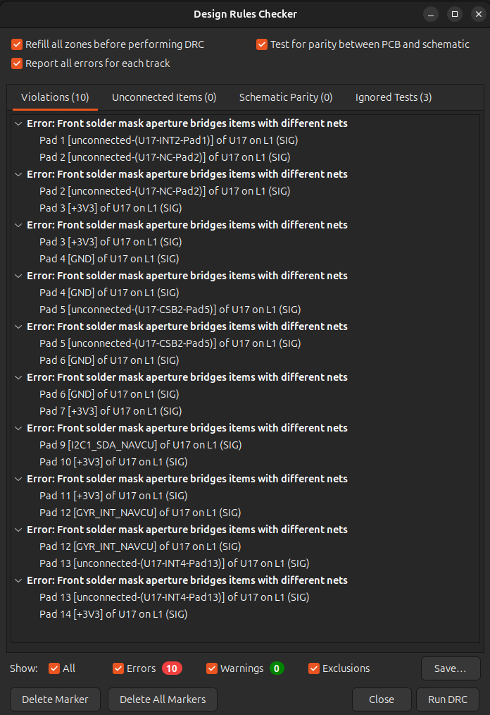
- The DRC Errors are known and it is due to the packagesize of the BMI088 (U17).
ERC
DRC
- 0 Errors if -> /File/Board Setup/Board Stackup/SolderMask&Paste/Allow bidged solder mask apertures between pads withing footprints
Known Issues
- TBD
Feel free to contact me if you notice any mistakes!
